FunO4StablePSCs
Functional Metal Oxides. Enhancing Stability and Efficiency of Perovskite Solar Cells
Project
Sun is arguably one of the most continuous sources of energy available at almost all living places of the world. Solar energy has the potential to provide clean and green energy for an unlimited time. Photovoltaics is a process to directly convert this source of energy into electricity. A solar cell is the basic device that is used to convert sunlight directly into electricity. There are many technologies utilizing these photovoltaic devices to generate electricity from the sun.
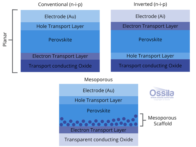
Perovskite Solar Cell (PSC) technology uses “Perovskite” structure layer to absorb solar irradiation and generate electron and hole charge carriers. The “Perovskite” absorber layer gets in-between charge transporting layers. These charge carriers are collected and then transported to external circuits through respective electron and hole transporting layers. These charge transport layers can contribute towards the efficiency and stability of Perovskite technology.
This project aims to:
- develop charge transporting layers that enhance efficiency and stability of the Perovskite absorber based solar cell technology;
- contribute to the stability of preferably Perovskite solar cell technology by improving the charge transporting layers, i.e., following an indirect approach to enhance stability and efficiency of the Perovskite Solar Cell Technology.


Research
The Perovskite Solar Cell technology has made a tremendous advancement over a very short period since its inception earlier this century. The PSC device, as goes with most of the photovoltaic devices, comprises multiple layers in its structure:
- absorber layer, the Perovskite, lies in between charge transporting layers
- an electron charge transport layer
- a hole charge transport layer
Then there are two electrodes at the outer sides for circulation of charges generated in the absorber and for the flow of current in the outer circuit.
The technology, otherwise promising and efficient, however lacks long-term durability and stability.
The lack of stability comes mainly from the instability of the active and absorber layer, i.e., Perovskite itself. When put in service outside the laboratory, the moisture, the UV irradiation and the surface reactions cause degradation of the absorber followed by the eventual degradation of the constituent layers.
This research project aims to contribute towards enhancing stability of the PSC device by indirect approach, i.e., addressing charge transporting layers.
The research project targets to develop transport layers from binary, tertiary, and quaternary functional inorganic metal oxides with enhanced characteristics.
The interfaces between the transport layers and the absorber Perovskite will be “engineered” through exploitation of “nanoscale” phenomenon arising out of “sizes” and “shapes”.
The research work will focus on development of transport materials that are efficient in charge extraction, transportation and have better energy band alignment to reduce charge recombination within layers and at the interfaces.
Outcomes
The research works will be periodically published in indexed journals and will also be shared in national/international conferences.
Team
Principal Investigator (PI)
Department of Molecular Sciences and Nanosystems (DSMN) - Ca’ Foscari University of Venice, Italy
Host Supervisor
Department of Molecular Sciences and Nanosystems (DSMN) - Ca’ Foscari University of Venice, Italy
Co-Supervisor
Department of Molecular Sciences and Nanosystems (DSMN) - Ca’ Foscari University of Venice, Italy
María Begoña Asenjo Zamorano
Collaborator
Energy, Environmental and Technological Research Center (CIEMAT) - Madrid, Spain
mbegona.asenjo@ciemat.es
Short bio - María Begoña Asenjo Zamorano
Begoña Asenjo, PhD in chemistry since 2007. She is an expert in Raman spectroscopy, and she has devoted her scientific career to the fabrication and characterization of materials for energy by using different chemical techniques (spin coating, chemical bath,electrochemical processes…) to photovoltaic solar energy (solar cells and modules), and recycling process.
Susana María Fernández Ruano
Collaborator
Energy, Environmental and Technological Research Center (CIEMAT) - Madrid, Spain
susanamaria.fernandez@ciemat.es
Short bio - Susana María Fernández Ruano
Dr. Susana obtained the graduate degree in Physics from the Complutense University of Madrid in June 1999. Subsequently, she obtained the PhD from the Department of Electronic Engineering at Polytechnic University of Madrid in October 2004. After that, she worked as a postdoctoral researcher on Ohmic contacts for GaN-based HEMTs under contracts with the Centre for Research and Development of the Navy (CIDA). In February 2007, she joined the Solar Photovoltaic Unit from the Energy, Environmental and Technological Research Centre (CIEMAT). Her main research focus is the development of a broad range of semiconductor materials by magnetron sputtering for energy applications, more specifically transparent conductive and metal transition oxides and non-hydrogenated amorphous silicon. Currently, she is the responsible of two magnetron sputtering systems devoted to the material fabrication.
Shrabani Panigrahi
Collaborator
Center for Materials Research (CENIMAT) - Department of Materials Science, New University of Lisbon, Caparica, Portugal
s.panigrahi@fct.unl.pt
Short bio - Shrabani Panigrahi
Dr. Shrabani Panigrahi is an accomplished physicist and FCT Post-Doctoral Research Fellow at the Universidade NOVA de Lisboa, Portugal. With over a decade of experience in experimental physics and materials science, her work focuses on the design, processing, and interfacial studies of solution-processed solar cells. Dr. Panigrahi’s expertise spans hybrid perovskite and oxide electronics, nanoscale characterization techniques, and device architecture modification for energy applications. She has published extensively in high-impact journals, contributing groundbreaking insights into photoconduction mechanisms and interfacial engineering. A highly skilled researcher, she has guided master and project students while excelling in collaborative, interdisciplinary environments.
José Pablo González
Collaborator
Energy, Environmental and Technological Research Center (CIEMAT) - Madrid, Spain
JosePablo.Gonzalez@ciemat.es
Short bio - José Pablo González
Dr. Jose Pablo holds a degree in Applied Physics. He has worked as a process engineer on semiconductor materials manufacturing lines. He is an expert in magnetron sputtering deposition, dry plasma etching (RIE), material processing, and characterization of thin films of various materials within the field of Renewable Energy.


